Coating and developing equipmentのメーカーや取扱い企業、製品情報、参考価格、ランキングをまとめています。
イプロスは、 製造業 BtoB における情報を集めた国内最大級の技術データベースサイトです。

Coating and developing equipment - メーカー・企業と業務用製品 | イプロスものづくり

Coating and developing equipmentの製品一覧

1~5 件を表示 / 全 5 件

表示件数

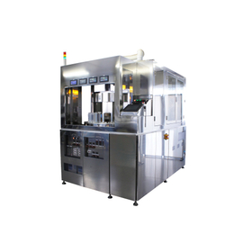
Automatic photoresist coating and developing equipment (coater-developer)

Compatible with low to high viscosity resists! We can manufacture equipment for any wafer size, from small diameter to large diameter!

【Features】 ■ Achieves low price ■ Supports low to high viscosity (1.7cP to 10000cP) ■ Compatible with sizes from 2 to 12 inches ■ Capable of processing multiple wafer sizes (e.g., compatible with 3, 4, 5 inches and 8, 12 inches) ■ Automatic wafer size recognition system ■ Proven performance with a variety of chemicals ■ Reduced footprint (space-saving) ■ Numerous options available with resist reduction ■ Lineup tailored to production volume 【ASAP Coater/Developer Functions】 ● Spin coating ● HMDS treatment ● Baking ● Cooling ● Developing ● Rinsing We have achieved low prices by handling everything from design to manufacturing and sales in-house! 【ASAP Features and Achievements】 ● Proven use of a variety of chemicals including positive and negative resists, polyimide, SOG, WAX, silicone, etc. ● Extensive experience in substrate transport including Si (silicon), GaAs, InP, GaN, SiC, sapphire, ceramics, SiO2 (glass), etc. ● Numerous transport achievements with thin substrates such as GaAs (thickness 150um), InP (thickness 150um), LT (thickness 120um)! *For more details, please refer to the PDF document or feel free to contact us.

  • Coater
  • Resist Device
  • Other semiconductor manufacturing equipment
  • Coating and developing equipment

ブックマークに追加いたしました

ブックマーク一覧

ブックマークを削除いたしました

ブックマーク一覧

これ以上ブックマークできません

会員登録すると、ブックマークできる件数が増えて、ラベルをつけて整理することもできます

無料会員登録

Coating and Developing Equipment ACS300 Gen2

Type up to 300mm - Spin Coating/Developing Cluster

Wafer-level packaging for mass production and 3D integration.

  • Other processing machines
  • Coating and developing equipment

ブックマークに追加いたしました

ブックマーク一覧

ブックマークを削除いたしました

ブックマーク一覧

これ以上ブックマークできません

会員登録すると、ブックマークできる件数が増えて、ラベルをつけて整理することもできます

無料会員登録

Tokyo Electron Kyushu Product Catalog

Featuring the latest products from Tokyo Electron Kyushu, a leading company in semiconductor manufacturing equipment!

The "Tokyo Electron Kyushu Product Guide" is a comprehensive catalog from Tokyo Electron Kyushu, which conducts research, development, and design of semiconductor manufacturing equipment and EPD manufacturing equipment. It features a number of the latest semiconductor coating and developing equipment along with detailed explanations. Additionally, it introduces trends in the current semiconductor coating and developing equipment research projects, as well as the development projects for semiconductor cleaning equipment. Currently, the product guide is being offered for free. [Contents] ■ Semiconductor Coating and Developing Equipment ■ Semiconductor Cleaning Equipment ■ Wafer Bonding Equipment ■ FPD Coater ■ Introduction to Research and Development of Various Semiconductor Manufacturing Equipment *For more details, please refer to the catalog or feel free to contact us.

  • Other semiconductor manufacturing equipment
  • Coating and developing equipment

ブックマークに追加いたしました

ブックマーク一覧

ブックマークを削除いたしました

ブックマーク一覧

これ以上ブックマークできません

会員登録すると、ブックマークできる件数が増えて、ラベルをつけて整理することもできます

無料会員登録

Automatic resist coating and developing equipment for corner substrates (coater-developer)

Supports low to high viscosity resist! Equipment can be manufactured for any wafer size!

The product is equipped with spin coating, HMDS treatment, baking, and cooling functions. Since we handle everything from design to manufacturing and sales in-house, we have achieved low prices! We have a proven track record with a variety of chemicals including positive-negative resist, polyimide, SOG, wax, and silicone. We also have extensive experience in transporting various substrates such as Si (silicon), GaAs, InP, GaN, SiC, sapphire, and ceramic, as well as SiO2 (glass). We have numerous achievements in transporting thin substrates and square substrates, such as GaAs (thickness 150um), InP (thickness 150um), and LT (thickness 120um)! 【Features】 ■ Achieves low prices ■ Capable of handling low to high viscosity (1.7cP to 10000cP) ■ Uniform film distribution through a rotating cup coating method ■ Compatible with 2 to 12 inches ■ Capable of processing multiple types of wafers (compatible with 3, 4, and 5 inches) ■ Automatic recognition of wafer size ■ Proven track record with a variety of chemicals ■ Reduced footprint (space-saving) ■ Numerous options for resist reduction ■ Lineup tailored to production volume *For more details, please refer to the PDF document or feel free to contact us.

  • Coater
  • Coating and developing equipment

ブックマークに追加いたしました

ブックマーク一覧

ブックマークを削除いたしました

ブックマーク一覧

これ以上ブックマークできません

会員登録すると、ブックマークできる件数が増えて、ラベルをつけて整理することもできます

無料会員登録

Coating and Developing Equipment ACS200

Fully automatic, compatible with a maximum of 200mm.

By docking our mask aligner module with the full-area exposure method, it can be used as the Ring Graphy Cluster LithoFab200.

  • Other processing machines
  • Coating and developing equipment

ブックマークに追加いたしました

ブックマーク一覧

ブックマークを削除いたしました

ブックマーク一覧

これ以上ブックマークできません

会員登録すると、ブックマークできる件数が増えて、ラベルをつけて整理することもできます

無料会員登録